Materialien für die Nanosensorik - Fraunhofer ENAS, Department Back End of Line (BEOL) - TU Chemnitz
←
→
Transkription von Seiteninhalten
Wenn Ihr Browser die Seite nicht korrekt rendert, bitte, lesen Sie den Inhalt der Seite unten
Materialien für die Nanosensorik
                                      Jörg Schuster

                  Fraunhofer ENAS, Department Back End of Line (BEOL)

                              joerg.schuster@enas.fraunhofer.de

Schuster
Seite 1
Fraunhofer ENAS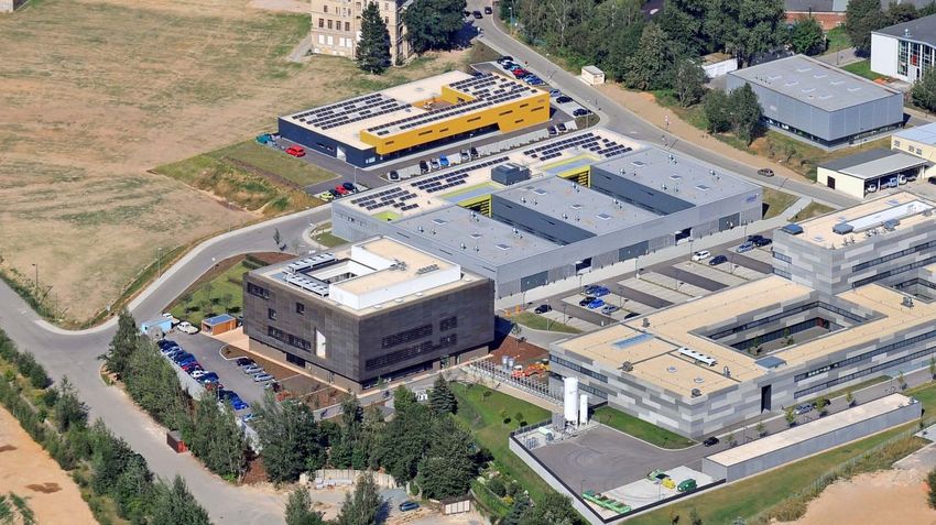
Fraunhofer Institute for Electronic Nanosystems
Systems integration by using of micro
and nano technologies
MEMS/NEMS design
Development of MEMS/NEMS
MEMS/NEMS test
System packaging/waferbonding
Back-end of Line technologies for
International Offices of Fraunhofer ENAS: micro and nano electronics
Since 2001/2005 Tokyo/Sendai, Japan Process and equipment simulation
Since 2012 Project-Center in Sendai Micro and nano reliability
Since 2002 Shanghai, China Printed functionalities
Since 2007 Manaus, Brazil Advanced system engineering
Schuster
Seite 2
Fraunhofer ENAS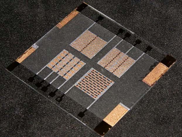
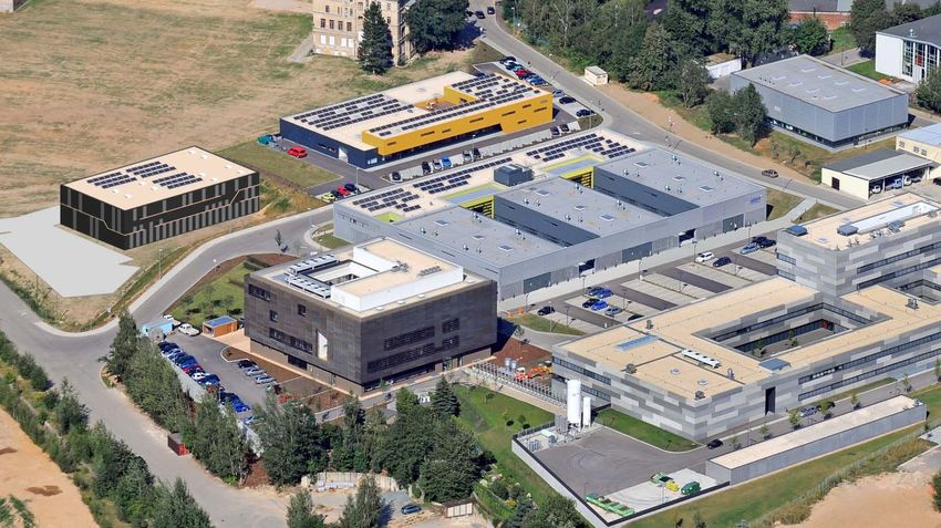
Microflex Center Chemnitz          3D-Micromac AG       Lightweight Structures Engineering
3D-Micromac AG, Fraunhofer ENAS

                                                                           Start-up-building

Fraunhofer ENAS         Institute of Physics and Center for Microtechnologies at the CUT
   Page 3
   Fraunhofer ENAS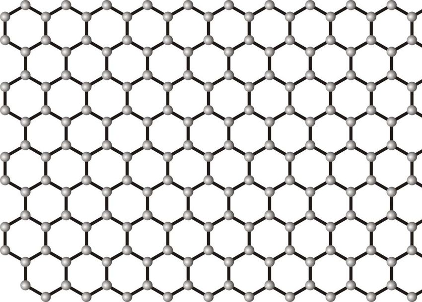
Smart Systems from the Device Point of View

                                          Inte
                                              grat
                                                  ion
      Processor                          Pac  &
                                             kag
                                                ing
               &    Radio
        Memory
                                                      Commu-
                   Sensor       MEMS /                nication
                                NEMS                  Unit
          Power       &                  Electronic
                                         Components
                   Actuator

Prof. T. Gessner
Page 4
Fraunhofer ENAS
Trends in der Nanoelektronik

Seite 5
Fraunhofer ENAS
Nanosensorik?

           MEMS = Micro Electro Mechanical System (z. B. Inertialsensoren)
           NEMS = Nano Electro Mechanical System

                     • Kleiner, aber stark wachsender Markt
                     • Zukunftstechnologie

Schuster
Seite 6
Fraunhofer ENAS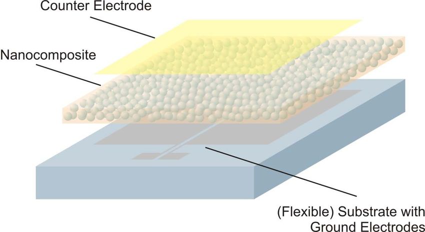
Nanosensorik?

• Nanoskalig (typ. < 100 nm)
• Größenabhängige Eigenschaften
• Quanteneffekte
• Extrem Strukturabhängige Eigenschaften

 Top down                         Bottom up
 - Lithografie, Si-Technologie    - Nanotechnologie, Selbstorganisation

  Schuster
  Seite 7
  Fraunhofer ENAS
Nanosensorik?

Chemisch
- Erkennung von Molekülen
- Oftmals Schlüssel – Schloss-Prinzip
- Selektivität!                          Viele biologische Systeme
- optisches oder elektronisches Signal   stellen funktionierende
                                         chemische Nanosensoren dar.

Physikalisch
- Physikalische Größen (Druck,
Temperatur, Beschleunigung, Licht)

Schuster
Seite 8
Fraunhofer ENAS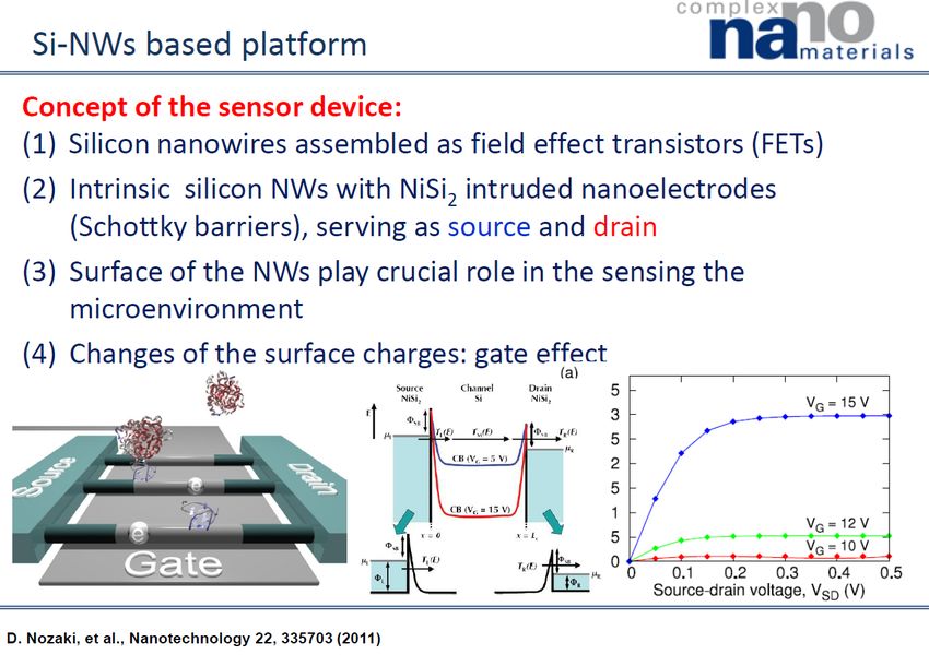
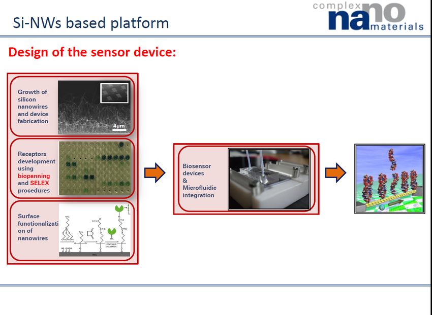
Nanomaterialien?

Nanostrukturen
- Strukturierung (Si-Nanodrähte)
- Synthese (Kohlenstoffnanoröhrchen,
Halbleiternanokristalle)

Nanokomposite
- Nanoskalige Komponente in
kontinuierlicher Matrix

Schuster
Seite 9
Fraunhofer ENAS
Silizium Nanodrähte

                  Larysa Baraban, Cuniberti group, TU Dresden

Schuster
Seite 10
Fraunhofer ENAS
Schuster Seite 11 Fraunhofer ENAS
Schuster
Seite 12
Fraunhofer ENAS
Current Topics of the Group

      Optical and Nanocomposite-based
                   Systems
                          Jörg Martin

Jörg Martin
Page 13
Fraunhofer ENAS
Integration of Nanomaterials Humidity Sensors
Schematic setup of composite sensor
H2O
Ceramic Particles
Mesurement principle
adsorption of water mole-
cules on particles
increase of dielectric
constant
sensitive particles: ceramics
change of capacity
polymer matrix: PMMA
Jörg Martin
Page 14
Fraunhofer ENASIntegration of Nanomaterials Humidity Sensors
change of sensor capacity up to
nearly 130 %
Capacity change as function of humidity
150
00%%SiOCeramic
2 Particles
of capacity (%)
125 2020
%%SiOCeramic
2 Particles
40 % SiO2
Kapazitätsänderung (%)
40 % Ceramic Particles
100 60 % SiO2
60 % Ceramic Particles
10 mm
75
50
Change
response times in the range 25
of 15 – 20 sec
0
comparable with commercial sensors
20 30 40 50 60 70 80
Rel. Luftfeuchte
Relative humidity (%)
(%)
Jörg Martin
Page 15
Fraunhofer ENASSemiconductor Nanocrystals
fluorescence = recombination of electron-
hole-pairs (excitons)
photon energy depends on size 5
4
Bandgap (eV)
P. F. Trwoga, et al., J. Appl. Phys. 83, 3789 (1998).
3
2
1 2 3 4www.invitrogen.com
5 6
Particle Diameter (nm)
Wavelenght (and other parameters)
depend on size of the particles.
Jörg Martin
Page 16
Fraunhofer ENASOverview
Semiconductor Nanocrystals
Special photophysical properties
Quantum Confinement
Sensitivity against electrical charges
Usage as light emitters Usage as Nanosensors
LEDs, displays Optical detection of
fluorescence markers charges and electrical fields
Jörg Martin
Page 17
Fraunhofer ENASLoad Detection with Nanocrystals
Nanocrystal Layer
Piezoelectric Foil
Lightweight Structure
Force
Jörg Martin
Page 18
Fraunhofer ENASSpintronik – Erzeugung und Untersuchung
spintronischer Schichtsysteme
Laufzeit: 3 Jahre seit 01.01.2011
Partner: TUC – Professor Albrecht
HSMW – Prof. Exner
HSMW – Prof. Weißmantel
ENAS – Prof- Stefan Schulz
Ziel: 3achsiger GMR-Sensor
Ramona Ecke
Page 19
Fraunhofer ENASSpintronik - Grundlagen
Magnetwiderstand = Verhältnis des Widerstandes eines Materials ohne und
mit externem Magnetfeld
GMR = Riesenmagnetwiderstand
in Vielfachschichtsystemen mit dünnen ferromagnetischen und
nichtmagnetischen Schichten (Fe/Cr)
Anlegen eines Magnetfeldes – Widerstandsänderung
R↓ = ferromagnetische (parallele) Austauschkopplung
R↑ = antiferromagnetische (antiparallele) Austauschkopplung
Ramona Ecke
Page 20
Fraunhofer ENASSpintronik – Grundlagen der Schichtsysteme
Klassisch Spin-Valve Spin Valve mit AAF
• 2 magnetische (M)
Schichten durch eine durch
eine nichtmagnetische
(NM) getrennt
• Dicke der NM so, dass
sich ohne Magnetfeld eine • NM so dick, dass keine magn. • vergleichbar mit Variante 2, aber
antiferromagnetische Kopplung untere M ist ein künstlicher
Kopplung einstellt • Untere M stark an antiferromagn. Antiferromagnet
• äußeres Magnetfeld Schicht gekoppelt Hard Layer höhere Temperaturstabilität
erzwingt parallele • obere M weichmagnetisch Reduzierung von Hysterese-Effekten
Ausrichtung der Ummagnetisierung durch äußere
Magnetisierung R Magnetfelder R-Änderung
Ramona Ecke
Page 21
Fraunhofer ENASDisplacement detection with CNTs
integrated in NEMS
Sascha Hermann, Sergei Loschek,
Stefan E. Schulz,
Contact
Dr. Sascha Hermann
Group leader “CNT Integration and Application”
Fraunhofer Institute for Electronic Nano Systems (ENAS)
Sascha.hermann@enas.fraunhofer.de
Tel.: +49 371 531 35675Motivation
Capacitive silicon based MEMS for displacement detection
30 µm 30 µm
MEMS acceleration sensor MEMS gyroscope
Dienel, Dissertation, TU Chemnitz, 2009
Page 23
Fraunhofer ENAS
Sascha HermannIntroduction: CNT-Structure
Visualization of a CNT:
“roll-up of graphene sheet”
a1
a2
Θ
Single-Walled Carbon Nanotube (SWCNT)
C = na1 + ma2
- Graphene sheet: sp2 hybridized C atoms
- Definition of CNT by (n, m) Multi-Walled Carbon Nanotube (MWCNT)
Page 24
Fraunhofer ENAS
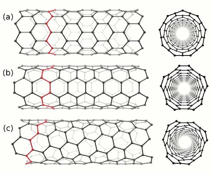
Sascha HermannIntroduction: CNT-Structure
zigzag
e.g. (9,0)
armchair
e.g. (5,5)
chiral
e.g. (7,3)
• Possible SWCNT types:
− semiconducting
− semimetallic
− metallic
• MWCNTs are metallic (n,m)
Page 25
Fraunhofer ENAS
Sascha HermannTransducer principles Piezoresistive transducer principle Field emitting transducer principle Strain of a semiconducting SWCNT A displacement changes electrical changes the band gap. field strength on the CNT tip. Page 26 Fraunhofer ENAS Sascha Hermann
Preparation of CNT dispersion
CNT dispersion for the                                    Dry                    CNT dispersion for the
piezoresistive transducer                                                        Field emitting transducer

                                                   Dispersion

              Semiconducting                                                       Metallic               MWCNTs
                SWCNTs                                                             SWCNTs

                      Dispersions with defined properties:
                      • Non-covalent functionalization
                      • Preparation procedures for mild separation but high separation grade
                      • Use of preselected SWCNTs (type/chirality)
                      • Use of length restricted CNTs

                                      Yu, H.; Hermann, S.; Schulz, S.E.; Geßner, T.; Dong, Z.; Li, W.J.: “Optimizing Sonication
                                      Parameters for Dispersion of Single-walled Carbon Nanotubes” Chem. Phys. (in press)

    Page 27
    Fraunhofer ENAS
    Sascha Hermann
Integration method for displacement sensors: Examples
• CNT deposition and
alignment on 6” wafers
demonstrated
15 µm 2 µm
• Integration of Pd
electrodes
• CNT density can be
controlled
• Coupling DEP for large
CNT arrays
• Assembly of metallic,
semiconducting SWCNTs
and MWCNTs
15 µm 2 µm
Page 28
Fraunhofer ENAS
Sascha HermannMEMS tool for test and characterization of CNT transducer
Piezoresistive transducer principle Field emitting transducer principle
CNT strain CNT to electrode displacement
Contact reliability Field emission properties
Page 29
Fraunhofer ENAS
Sascha HermannPiezoresistive Effect of CNTs
Chirality dependent
piezoresistive effect
(6,2) CNT semiconducting Low diameter,
(7,4) CNT semimetallic
(6,6) CNT metallic High curvature
Overlap of π-orbitals
Band gap [eV]
Analytical model
DFT required! (Tight binding)
Improved analytical model
for high diameter CNTs
Strain [%]
Piezoresistive effect for (nearly) all CNTs available by DFT or AM
Florian Fuchs, Bachelor thesis, ENAS/TUC 2012 C. Wagner, JS et al., phys. stat. sol. B, in press
Schuster
Seite 30
Fraunhofer ENASNanomodels for Sensor System Simulation Piezoresistive effect
Band gap by DFT or AM Simple resistivity model
sensor window
C. Wagner, JS et al., phys. stat. sol. B, in press
Schuster
Seite 31
Fraunhofer ENASDFG Research unit 1713: Sensoric Micro- and Nanosystems (SMINT)
Design of components Simulation of CNTs for
FEM-Model and systems based on sensor application
new technologies
Development of Integration of
new materials Components and
and technologies systems Opto-fluidic sensor
Nanocharacterization element
Array of rolled-up-
Array of magnetic 1,5 µm
tubes Functionalization of CNTs for
multilayer nano caps MOS-Detection
sensors and interconnectsENAS, TUC, HSMW, …
Nanosystemintegration, u.v.m.
Zentrum für
Materialien, Architekturen und
Integration von Nanomembranen
(MAIN)
TUC, ENAS, IFW DD
ENAS, TUC ENAS, TUC, TU DD
ENAS, FhG, …
Nanosensoren in CNT-Nanoelektronik, u.v.m.
Leichtbaumaterialien, Sensorik, Aktorik,
u.v.m. u.v.m.
Schuster
Seite 33
Fraunhofer ENASSie können auch lesen