Photonics in Germany in Germany 2019 - Optische Technologien in Deutschland - Cluster Optik und Photonik
←
→
Transkription von Seiteninhalten
Wenn Ihr Browser die Seite nicht korrekt rendert, bitte, lesen Sie den Inhalt der Seite unten
Photonics
                    Photonics
                  in Germany
                  in Germany
                         2019

Optische
Technologien
in Deutschland

                       Optische
                   Technologien
                 in Deutschland
Connecting Global Competence

                                                O N
                              T I
                          V A         H T
                       N O      L I G     9
                                         1
                    IN     ITH ER 2     0
                         W OB
                                      C T
                                N   O
                            U I
                       YO
                SE   E

                                    OCTOBER 17–19, 2019, BEC, MUMBAI
                                    India’s Platform for Laser and Optical Technologies—
                                    Components, Systems and Applications
 © Fraunhofer HHI

world-of-photonics-india.com
INHALTSVERZEICHNIS

                                        1

                     © Fraunhofer ILT
2

    Table of Contents

                 Preface                                              Innovations in Growth Markets
                 Grußwort                                             Innovationen in Wachstumsmärkten

      4
      Frau Anja Karliczek,                                18   Sebastian Rhode et al., Carl Zeiss Microscopy
      Member of the German Bundestag,                          GmbH
      Federal Minister of Education and Research               Advanced Segmentation for Research and Indus-
    		Mitglied des Deutschen Bundestages                       try Applications using Machine-Learning
      Bundesministerin für Bildung und Forschung          22   Stephan Ritter, Jürgen Stuhler,
                                                               TOPTICA Photonics AG
                                                               Lasers in the Quantum World
                                                          26   Julia Baldauf et al., CiS Forschungsinstitut für
                                                               Mikrosensorik GmbH; Steffen Biermann,
                 Location Germany                              Micro-Hybrid Electronic GmbH
                 Standort Deutschland                          Fabrication and Packaging of Infrared
                                                               Emitting Devices
      8   Gerhard Hein, VDMA                              28   Simon Britten, Laserline GmbH
          Germany's Strengths as a Business Location           Blue Wavelength Meets High Power Diode
    10    Frank Schlie, BMBF                                   Lasers – Enabling Tool for Copper Prozessing
          Digital Change Driven by Photonics              30   Thomas Schopphoven, Andres Gasser,
          and Other Quantum Technologies                       Fraunhofer ILT; Gerhard Backes, RWTH Aachen
    12    Max Milbredt, Germany Trade and Invest               Environmentally Friendly Alternative to Hard
          International Investment in Germany’s                Chrome Plating and Thermal Spraying
          Photonics Industry                              32   Philipp Wagenblast, TRUMPF Laser- und System-
    14    Jörg Mayer, Spectaris                                technik GmbH
          Why the Photonics Manufacturing Industry will        The Importance of Photonics in Additive Manufac-
          Remain a Domestic Value Generator, Unlike the        turing
          Photovoltaics Industry                          34   Andreas Vogelpoth, Fraunhofer ILT;
                                                               Jochen Stollenwerk, RWTH Aachen
                                                               Additive Manufacturing: Laser Powder
                                                               Bed Fusion with VCSEL Heating
3
Inhaltsverzeichnis
36 Dirk Hauschild, LIMO GmbH Innovations and Competencies
Wafer-based Mass Production of High-precision in Industry
Glass Optics for Diode Laser Applications Innovationen und Kompetenzen
38 Thomas Knieling et al., Fraunhofer ISIT aus Unternehmen
Optical MEMS-Scanner: Design,
General Drives and Applications 62 Berliner Glas KGaA Herbert Kubatz
40 Ole Peters, Menlo Systems GmbH; Datong Wu, Mu- GmbH & Co.
nich University of Applied Sciences 63 Dausinger + Giesen GmbH
Investigating Ceramic Coatings with 64 Heraeus Quarzglas GmbH & Co. KG
Terahertz Radiation 65 Instrument Systems GmbH
42 Jim Zou, Mirko Lawin, 66 Laserline GmbH
ADVA Optical Networking SE 67 LT Ultra-Precision Technology GmbH
Optical Transceivers for 68 Omicron-Laserage Laserprodukte GmbH
5G Mobile X-haul Applications 69 OSRAM Opto Semiconductors GmbH
44 Ute Neugebauer et al., Leibniz IPHT 70 OWIS GmbH
Photonic Solutions for Medicine and Environment 71 SENTECH Instruments GmbH
46 Joachim Reill, OSRAM Opto Semiconductors
GmbH
Optoelectonic Innovation Drives the Next
Generation of Intelligent Vehicles
48 Ramona Eberhardt, Fraunhofer IOF Networks and Markets
Freeform Optical Systems for Future Markets Netzwerke und Märkte
50 Steffen Reinl, JENOPTIK Optical Systems GmbH
Integrable Solutions for the Growth Market of 74 German Society of Applies Optics – Deutsche
Digital Laser Material Processing Gesellschaft für angewandte Optik e.V.
52 Jürgen Geffe, Vision & Control GmbH 76 THE GERMAN CAPITAL REGION excellence in pho-
vicotar® Blue Vision Compact, Robust, tonics
Lightweight – Telecentric Measurement Lenses 78 LASER World of PHOTONICS
for the Blue Spectral Range 80 Impressum
Results and Services
from Research Institutions
Ergebnisse und Dienste
von Einrichtungen der Forschung
56 Fraunhofer IOF
58 Fraunhofer ILT
4
Preface Anja Karliczek
Federal Minister of
Education
and Research
Bundesministerin für
Bildung und Forschung
Whether we think of bright summer evenings or candlelight Photonics also provides essential assistance in industrial
and fireside in winter, we associate light with pleasure and production, for example when laser systems separate or
warmth. But light can do so much more. We can concen- join various components or when production processes
trate it on a millionth of a millimetre. We are capable of high are monitored. And one last example: Autonomous driving,
technological feats, creating up to billions of megawatts. which needs complex optical sensors. We already know
And nothing moves faster than light. how they work in car parking assistants which beep when
we move too near another car.
Photonics helps us take advantage of these properties of
light. Photonics is an important key technology that many All this makes photonics an important sector which has cre-
areas can no longer do without. Just think of medicine: ated more than 130,000 jobs. At the same time, photonics
Whether X-rays or computer tomography – imaging tech- is a major driver of innovation for digital transformation.
niques often provide the basis for precise diagnosis. And Germany needs innovations which serve the people while
minimal invasive surgery is only possible thanks to small increasing prosperity and growth. This helps us remain
cameras that serve as the surgeon's eyes inside the pa- competitive on the international stage. Photonics makes a
tient's body. Photonics "made in Germany" is used for this substantial contribution to this, as the brochure "Photonics
purpose. It helps to restore people's health. in Germany" impressively shows. Enjoy the read!
Anja Karliczek
Member of the German Bundestag
Federal Minister of Education and Research
5
Grußwort
Egal ob wir an lange helle Sommerabende denken oder an Auch in der industriellen Produktion leistet Photonik
gemütliche Stunden bei Kerzenlicht und Feuerschein im Win unerlässliche Hilfestellungen, wenn etwa Lasersysteme ver
ter – Licht gilt uns als Quelle von Freude und Wärme. Licht schiedene Teile trennen beziehungsweise zusammenfügen,
kann aber noch viel mehr. Wir können es auf den millionsten oder wenn es um die Überwachung von Fertigungsprozessen
Teil eines Millimeters fokussieren. Wir können technologisch geht. Und ein letztes Beispiel: autonomes Fahren, das eine
Höchstleistungen erzielen, bis zu Milliarden von Megawatt. komplexe optische Sensorik benötigt. Wie sie wirkt, merken
Und nichts ist schneller als Licht. wir schon jetzt, wenn der Parkassistent laut piept, weil wir
einem anderen Auto zu nahe gekommen sind.
Mit Hilfe von Photonik nutzen wir diese Eigenschaften All das macht Photonik zu einer bedeutenden Zukunfts
von Licht. Sie ist eine wichtige Schlüsseltechnologie, die aus branche. Mehr als 130.000 Menschen arbeiten in diesem
vielen Bereichen nicht mehr wegzudenken ist. Nehmen wir Bereich. Photonik ist gleichzeitig ein wichtiger Innovations
nur die Medizin: Ob Röntgenaufnahmen oder Computerto motor für die Digitalisierung. Deutschland braucht solche
mographie, bildgebende Verfahren stehen oft am Anfang Innovationen, die dem Menschen dienen und gleichzeitig
einer präzisen Diagnose. Und minimalinvasive Eingriffe sind Wohlstand und Wachstum mehren. So bleiben wir interna
nur deswegen machbar, weil es kleine Kameras gibt, die für tional wettbewerbsfähig. Die Photonik leistet dazu einen
den Chirurgen zu Augen im Körperinneren werden. Photonik wichtigen Beitrag. Die Broschüre „Photonics in Germany“
„made in Germany“ wird hierfür genutzt. So hilft sie, Men macht dies auf eindrucksvolle Weise deutlich. Ich wünsche
schen gesund zu machen. allen Leserinnen und Lesern eine spannende Lektüre.
Anja Karliczek
Mitglied des Deutschen Bundestages
Bundesministerin für Bildung und Forschung
Standort
Deutschland

© TOPTICA Photonics

Location
Germany
LOCATION GERMANY

8

    Germany's Strengths
    as a Business Location

                                                                                        Gerhard Hein,
                                                                                          VDMA Laser
                                                                                   and Laser Systems
                                                                              for Material Processing,
                                                                                     Photonics Forum

    Germany is a leading hub for business and diversified re-        quirements of individual user industries, process robust-
    search. With its rational regulatory framework and system-       ness and high availability as well as integrated services.
    atic research funding that is oriented towards feasibility but   Industrial software and monitoring solutions are gaining in
    at the same time open to future-oriented foundations, it is      significance, specifically the visualisation of current condi-
    a guarantor of innovativity. Research funding is of particular   tions and the prediction of possible failures using trend and
    importance in Germany: in many cases it results from indus-      pattern recognition. The main challenges in the future will
    try-oriented agenda processes or is based on an holistic ap-     be the linking of additive manufacturing with the objectives
    proach and follow-up measures which cover all programme          of Industry 4.0, networking across all process steps and
    content and collaborative projects over time. Particular         the establishment of standard industrial processes in the
    importance is attached to the fact that the market-driven        area of "Additive Manufacturing" (AM).
    development concerns of industry are addressed, while the
    expertise of highly qualified institutes – especially with re-   Differentiated consideration of opportunities and
    gard to preliminary research – is taken fully into account.      demands now required
                                                                     This applies in rather general form to the set of principal
    The funding guidelines of the Federal Ministry of Education      goals. Of course, it could be left to the equipment manufac-
    and Research on "Line integration of additive manufactur-        turers themselves to overcome obstacles to further market
    ing processes" provide a striking illustration of Germany's      penetration that have not yet been removed. These are
    strengths in this area. From a technical point of view, the      not difficult to identify, but are actually relatively difficult
    main objective is to make the transition from potent proto-      to deal with:
    type and small series production to productive series pro-           In small series production as well as in the production
    duction under exacting industrial conditions. This involves      of complex individualised components, cost advantages
    a huge increase in deposition rates, for example through         can certainly be obtained from additive processes without
    innovative multi-beam systems for the powder bed-based           tools. Considerable added value can be generated through
    LMF (Laser Metal Fusion) process, as well as complete so-        lightweight construction, internal cooling ducts or facilitat-
    lutions involving sophisticated concepts for parts and pow-      ing undercut contours. In such cases, it may also be pos-
    der management in order to increase machine utilisation          sible to eliminate cost disadvantages that are currently
    rates. New generations of multilaser systems now permit          enjoyed by medium and large series production.
    the production of competitive series components. However,            Of particular interest are also hybrid machines – for
    industrial solutions must cover the entire process chain         example laser deposition welding systems – which allow
    and take into account intelligent digitalisation, specific re-   specific processing functions of a different kind to be car-
                                                                     ried out during the build-up phase. However, this requires
                                                                     "3D printing"-compliant design and new approaches in
                                                                     production planning.
                                                                         In the case of large components, on the other hand,
                                                                     the focus is on the necessary increase in the build-up
                                                                     rates, the comparatively high prices of the systems them-
                                                                     selves as well as the limited variety of (suitable) material
                                                                     powders available. Added to these are the requirements
                                                                     of automated powder feeding, powder handling, powder
                                                                     disposal, dust pollution in the environment due to "un-
                                                                     packing" of the parts, process chains for the removal of
    Constructor of a Titanium Impellor. © DMG-MORI                   supporting structures, non-destructive quality testing of
STANDORT DEUTSCHLAND
9
the additive components and finally the proof of faultless controls were connected to various communication part-
reproducibility. ners for demonstration purposes.
The above production-related development require-
ments are acknowledged and are being addressed by Project-oriented versus basic research
reducing diffusion barriers and through the development There are currently signs of a reorientation in research
activities of plant, component and substrate manufacturers policy, both at the national and European level, towards
or research by renowned institutes. addressing future opportunities in the overall field of "quan-
tum technologies". In view of the foreseeable directional
Location-specific research policy correction in favour of increased support for basic research,
The coordinating and supportive research policy in Ger- backing should also be given to laser technology and pho-
many could not have yielded its current achievements if tonics being seen as important integral components of
the Ministry of Research and project sponsorships did not quantum technologies. Currently being intensively propa-
look beyond the immediate production technology. This is gated in connection with quantum technologies are sensor
where the aforementioned enhancement through support technology and highly sensitive imaging techniques, quan-
measures comes in: certification of additively manufac- tum computing with a focus on simulating highly complex
tured components, establishment of standardised AM pro- phenomena and overcoming the current limitations, as well
cesses, sustainable standards in the initial and further as communication technology including associated encryp-
training of workers, production planners, designers and tion aspects. Ongoing and planned activities are still very
university graduates in the form of additional qualifica- much laboratory-based, and potential market readiness is
tions through specialised advanced courses. The research unlikely to be reached within the next few years. Accord-
policy, industrial partners and sponsors of the highly ef- ingly, the VDMA, specifically its Laser and Laser Systems
fective German institutes (for which the country is justly Working Group and the Photonics Forum, advocate net-
envied worldwide) form a virtuous circle! Prime examples working physical research with engineering and the enabler
here include "transverse" research topics in the context function of important branches of photonics in the future.
of training requirements or standardization-related stud- The challenges lie in coordinating the research disciplines
ies on the selection of reference components for the pur- and creating transparency in terms of access to appropri-
pose of illuminating the entire chain. As far as standards ate infrastructures. The effects chain will be complex and
are concerned, a certain conflict arises due to the fact relatively costly, ranging from the equipment market for
that the application portfolio changes every six months laboratory technology to application development.
or so, or receives notable additions. Difficulties also arise
in machine acceptance, where particular components are
of great importance and relevant guidelines exist. Highly
promising applications are held back because they are dif-
ficult - or impossible - to reconcile with these guidelines.
The definition of approval criteria for a constant stream of
new applications is problematic!
No genuine line integration without connectivity
Last but not least, with the increasing implementability
of additive processes in industrial process chains, the
eventual emergence of customer demands will have to
be met by "connectivity" as a prerequisite for Industry
4.0 concepts. Semantics and parameters will need to
Additive Manufacturing. © DMG-MORI
be standardised in order to implement a universal, glob-
ally accepted interface based on the OPCUA Companion
VDMA – German Engineering Federation
Specification that can reliably and seamlessly integrate Verband Deutscher Maschinen- und Anlagenbau e.V.
machines and plants into customer- and user-specific IT Laser and Laser Systems for Material Processing
systems. The VDW association, which is responsible for Photonics Forum
Corneliusstraße 4
the machine tool industry and whose project also feeds
60325 Frankfurt am Main
into relevant VDMA activities spanning several mechani- Germany
cal engineering sectors, recently unveiled a "Universal
Machine Tool Interface" (umati) at the AMB trade fair in Phone +49 69 - 756081 - 43
Fax +49 69 - 756081 - 11
Stuttgart in October 2018 and successfully exhibited it Mail g.hein@vdw.de
on the stands of project partners. Different machines and Web photonik.vdma.orgLOCATION GERMANY
10
Digital Change Driven by Photonics
and Other Quantum Technologies
Photonics is an important key technology for Germany as a Guiding principles of technological change are:
location for innovation. It provides solutions for tomorrow's • the combination of individual photonic technologies
markets. Increasingly, photonics is driving digitization. Take to form integrated photonic systems; photonic micro
additive manufacturing, autonomous robots or vehicles integration,
– photonics provides an indispensable technology basis. • digital optics for applications ranging from medicine
This creates enormous opportunities for our companies. to industry 4.0 – from image capture via sensor-based
But the challenges are also immense: new competitors data evaluation and storage to data and image process-
are pushing their way into international markets. Classi- ing for user needs (multimodal imaging, computational
cal, discrete components are being replaced by highly in- imaging, 3D vision) as well as
tegrated photonic technologies; new production chains and • technologies, integrated systems and standards for
new business models are being created on the basis of photonic-based human-machine interfaces (gesture
photonic processes. It is necessary to shape this change, control, gaze control, near-field displays, 3D displays).
to optimally position the photonics industry for future tasks These challenges imply much more than application devel-
and growth markets, to join forces, to strengthen small and opment. It is about providing a comprehensive technology
medium-sized enterprises and to finance growth. base for future photonic system solutions - with enormous
Additive Manufacturing using Laser Metal Fusion (LMF). Image: TRUMPF GruppeSTANDORT DEUTSCHLAND
11
MinR Dr.
Frank Schlie,
Bundesministerium
für Bildung
und Forschung
sensor technology or secure commu-
nication.
The German Federal Ministry of Ed-
ucation and Research (BMBF) supports
collaborative research at the frontiers
of science and technology with closely
interlinked programs on photonics and
quantum technologies. The aim is to
establish and expand successful inno-
vation networks. We aim to be leaders
and partners for these future fields of
our industries.
The tasks in research and develop-
ment are immense, and the course is
First diode-pumped, intra-cavity frequency-doubled Nd:YAG laser (DPSS) now being set in international competi-
made of LEGO® bricks, Image: Prof. Dr. Mirco Imlau. tion - from basic research via systems
solutions in photonics and quantum
technologies to applications for in-
dustry and society. To be successful
here, we need science, research, in-
dustry and politics to work shoulder to
shoulder. Together, we must invest in
research and development. We need
to open our technologies as platforms
for inventors and makers. We will need
to attract the best minds and commit-
ted young talent - because innovation
is made by people.
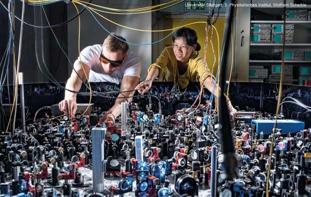
Photonics is a key enabler for Quantum Technologies, Image: Universität Stuttgart,
5. Physikalisches Institut, Wolfram Scheible
MinR. Dr. Frank Schlie
Bundesministerium für Bildung
significance for flexible production, medical and environ- und Forschung
mental technology and for networked infrastructures. Referat 515
At the same time, photonics lays the ground for com- Heinemannstrasse 2
53175 Bonn
pletely new fields of technology with enormous dynamics in Germany
the global competition in innovation. Today, photonic-based Phone +49 228 - 9957 - 3259
processes enable quantum technologies for ultra-precise Mail frank.schlie@bmbf.bund.deLOCATION GERMANY
12
International Investment
in Germany’s Photonics Industry
The photonics industry plays a central role in the devel- the fields of sales marketing, support or distribution. No
opment of a number of German economic sectors in the projects adding value to the products locally were record-
coming years; being driven by strong German companies, ed in the last five years.
internationally renowned R&D institutes and generous Germany is attractive as a location in the light sources
government support. business but with much less manufacturing activity than
But just how attractive is Germany’s photonic sec- in the last report. Both displays and light sources are
tor for international investors? In which fields are foreign largely destined for consumer markets. It can be seen
companies investing in in Germany? Are foreign direct that most of the FDI projects were primarily attracted to
investment (FDI) projects being carried out in areas where the large German consumer market, as opposed to estab-
the domestic industry has existing strengths? And how lishing projects to serve world markets from a manufac-
have the results changed compared to my last report? turing base in Germany. 38% of all light source projects
were sales, marketing and support acitivites from East
Compared with the last report 2 years ago, photovol- Asian companies tapping into the European and German
taics have significantly lost ground. This is because the markets.
temporary boom in investment caused by the German There is a clear trend towards FDI projects from China
feed-in tariff law is waning after 2012. A rapid drop in into Germany in recent years. In the photonics sector of
prices – caused by international competition – has caused measurement & automated vision most of the projects
investment in this segment to stall in recent times. Some- originated in classic industrialized countries. The US and
what surprisingly, light sources takes the top spot. Mea- Japan play the major roles in this category. This implies
surement & automated vision shows up in second place that the so-called triade of the US, Japan and Western
after hitting spot number 5 two years ago. Let’s examine Europe (Germany in particular) are still ahead of the com-
these two categories in more detail. petition from emerging markets in this field.
FDI projects in the field of displays were almost en- Production technology as well as medical technology
tirely carried out by Asian companies and exclusively in and life sciences have seen relatively few international
investment projects compared
to the levels of domestic produc-
tion. Possible reasons include
barriers to entry such as rigid
regulations (e.g. in life scienc-
es) or specific strengths of the
German industry making these
segments unattractive to new
entrants.
Measurement & automated
vision has received a significant-
ly higher share of FDI projects
compared to the last report. This
fact could hint at the big trend
of Industry 4.0 impacting inter-
Source: GTAI analysis based on FDI markets, November 2018 national interest and investmentSTANDORT DEUTSCHLAND
13
Max Milbredt,
Manager Investor Consulting
Electronics & Microtechnology
Germany Trade and Invest
ics sector can trigger the interest and commitment of
international investors.
To return to the initial questions, it is clear from ex-
amples like these that Germany’s photonics sector is at-
tractive to international investors. The German consumer
market for lighting and the sector of measurement & au-
tomated vision – possibly due to the rise of Industry 4.0
- are especially attractive for foreign investors. Germany’s
inherent strengths in medical technologies & life sciences
and production technology mean the country still has the
potential to attract foreign investment to its manufactur-
ing sector. Germany Trade & Invest actively approaches
international companies to encourage investment in all
Source: Photonics Industry Report
of these segments of the photonics industry in Germany.
About Germany Trade & Invest
Germany Trade & Invest provides free consulting services
to photonics companies looking to invest in the country.
We consult on all matters concerning the market: from tax
and legal issues and investment funding through to site
identification. Germany Trade & Invest is funded by the
Federal Ministry for Economic Affairs and Energy (BMWi).
* The Financial Times fDi Markets foreign direct investment
database was used to derive the data for this article.
The sector definitions are based on those used in the
Photonics Industry Report 2013 (jointly published by the
German Federal Ministry of Education and Research and
the SPECTARIS, VDMA, and ZVEI German trade associati-
Source: GTAI analysis based on FDI markets, November 2018 ons).146 FDI projects were identified for the six-year peri-
od from January 2011 to December 2015.
into Germany in this field. The share of projects has risen
to 19% from 8% just two years ago.
Max Milbredt
One particularly interesting example of an invest- Manager Electronics & Microtechnology
ment in photonics technologies in the period examined Germany Trade and Invest
was Samsung’s investment in Novaled in 2013. Novaled, Gesellschaft für Außenwirtschaft
und Standortmarketing mbH
based in the eastern German city of Dresden, is a manu-
Friedrichstraße 60
facturer of OLED materials. These materials are used in 10117 Berlin
novel applications such as OLED televisions and OLED Germany
lighting. The investment was one of Germany’s most suc- Phone +49 30 - 200 099 - 408
Fax +49 30 - 200 099 - 111
cessful venture capital exits to date, and a prime example Mail max.milbredt@gtai.com
of how new technologies developed in Germany’s photon- Web www.gtai.comLOCATION GERMANY
14
Why the Photonics Manufacturing Industry
will Remain a Domestic Value Generator,
Unlike the Photovoltaics Industry
A German view on the nature of high-tech photonics
Germany is seen as a leader in various technologies, 2018. Although it harboured great hopes at the start, the
strong in innovation and academics but weak in exploiting large-scale German PV industry experienced a short life-
its leadership in large-scale market uptakes. Take televi- cycle, basically in a time lapse compared to the lifecycles
sion technology, mobile phones or semiconductors. In none of other industries.
of these segments Germany transferred its innovative ca-
pacity into sustainable big business. Why photonics is different
Is there reason to assume that the photonics industry The industrial application of light – photonics – that
could face a similar fate? In the search for a plausible emerged around the same time as PV, has so far been
prognosis, it helps to look at an industry that not only has a spared from similar developments. Or is it merely experi-
similar name, but also operates with similar technologies: encing similar progress in slow motion? Are global competi-
Photovoltaics (PV). tion, increasing price pressure, and market concentration
Considerable market uptake was not seen before the also endangering this industry?
late 1990s. Fuelled by the societal desire to introduce Let us first look at what photonics constitutes. Photon-
measures for climate protection and non-nuclear energy ics is not a singular technology, but instead serves as an
supplies, government support was introduced, which guar- umbrella term for a series of different optical technolo-
anteed a fixed payment for every injected kilowatt hour. gies such as the light sources lasers/LED/OLED, imaging
Hence, the demand rose significantly. By the mid-2000s, optics, fibre optics, optical sensors, displays, and – here
capacities for manufacturing PV modules emerged close to we are again – solar cells. All these technologies trigger
where the demand was, meaning mainly in Germany. But great leverage effects in their application areas. They con-
the industry was too slow in adapting its capacities and tribute to the value of the end product or service, either by
development efforts to the growing global demand. In this enabling/enhancing the productivity of the manufacturing
seller’s market, many producers were lulled into a false process, or by providing/enhancing functionality in the end
sense of security. The Chinese government recognised the device. Example: to produce optical and electronic prod-
potential of the rising number of guaranteed markets and ucts, prognoses indicate that nearly 80% of revenues will
a trend towards national energy transitions. In its 12th depend on photonics in 2020 as analysts say.
Five-Year Plan from 2011, it named PV as a key technol- The steady development and growth of these appli-
ogy and thereby laid the foundation for massive domestic cations is forcing photonics itself to conduct intensive
growth in manufacturing. For years, this industry’s produc- research and development activities. Not least because
tion far exceeded domes-
tic demand, as a result
of which the excess was
distributed at low prices
to markets that yielded
stable returns. Europe-
ans could not withstand
this price pressure. Af-
ter a transition period
with punitive tariffs on
Chinese imports, even
the last major German
manufacturer was forced
to throw in the towel inSTANDORT DEUTSCHLAND
15
Jörg Mayer
Managing Director
SPECTARIS
driving. Lasers for material processing
or optical storage are also delivering
favourable growth prognoses.
German Photonics must prove that
it can master the growth. Other coun-
tries can scale up much more rapidly,
as the example of PV has shown. The
first area to consider is the availability
of specialists and academics, which
could otherwise be the greatest inhib-
iting factor to the upswing. The German
university system is reacting quickly,
partly driven by the federal structure in
of this can photonics be described as a key enabling Germany which seeks to generate locational advantages
technology. through specific research and cluster programmes. Today,
In Germany, photonics has recently steered onto an about 20 university locations offer a degree in the field of
impressive road to success. After generating turnover of lasers and optics. Although the PV industry produced an-
€31 billion in 2016, this value is expected to rise by more nual revenue of €14 billion (2011) at its peak, comparable
than 22% to €38 billion by the end of 2018. In the same numbers are considerably lower.
period, the number of employees in Germany is anticipated However, a dense education landscape is not the only
to grow to nearly 140,000 - an increase of 13%. benefit. Development partnerships are a major advan-
When observing the product segments that deliver both
a high production volume in Germany and high growth rates
at the same time, optical components and parts, analysis
and measuring technology, production technology, as well
as medical technology stand out. Since these segments
hold a strong German position in the global market with a
consistent share of more than 15% of the global produc-
tion, photonics is maximising its value contribution to the
domestic value chain.
Is the German position sustainable?
China is catching up. While Japan and Europe have re-
corded a slightly declining share of the worldwide produc-
tion volume, China managed to reach nearly 30% of the
global production market share, following an upward trend.
However, it is expected that the overall global market will
increase from €530 billion (2017) to €800 billion by 2022.
Therefore, everyone will profit.
This development is driven by certain expanding markets.
These include automotive applications with optical compo-
nents, such as displays or LiDAR lasers for autonomousLOCATION GERMANY
16
And this brings us
back to the beginning:
PV was too late in rec-
ognising itself as more
of a commodity product.
The Asians recognised
this earlier and invest-
ed in comprehensive
production capacities
that were often based
on German plant engi-
neering and required a
relatively low number of
highly qualified employ-
ees. In addition, PV is
used in few fields that
purely deal with power
generation. Research
was able to focus on
increasing its efficiency.
tage, since complex optoelectronic and optomechanical Combined with achieving lowest unit costs, this resulted in
systems generally require a close-knit network of R&D a nearly irreversible competitive advantage.
and supplier companies, favoured by spatial proximity. It is not foreseeable that many photonics technologies
Respective networks are supported by associations such will turn into commodity products like PV did. Specialised
as SPECTARIS, which represent the interests of the pho- applications for medical or measuring technology will con-
tonics industry as well as various customer industries tinue to be driven by the technological advances of their
such as medical and laboratory technology. components and the successful collaboration of research
The German photonics industry knows: it can com- institutes, manufacturers, and users. This outlook fuels
pete in areas that deal with complex solutions or high- the hope that photonics as a key enabling technology will
precision products, in which a high customising or en- continue to have a home advantage for some time to come.
gineering effort is needed, and in those which focus
on individual production or small batches. These fields
particularly require engineers and qualified specialists
such as precision opticians and mechatronics engineers.
Germany has them!
But as soon as it comes to higher production amounts
and more standardised products that have a greater fault
tolerance, German companies struggle to keep up. Light SPECTARIS German Industry Association for Medical Tech-
technology, light, and sensors in car manufacturing, opti- nology, Optical Technologies, Analytical, Biological, Labora-
tory, and Ophthalmic Devices
cal sensors in the consumer area, e. g., for smartphones, Jörg Mayer
live off high volumes. Here, other locational factors such Managing Director
as higher labour costs and bureaucratic hurdles prove Werderscher Markt 15
10117 Berlin
to be disadvantageous. A high degree of automation on
Germany
par with Industry 4.0 may offer a solution, but one which Phone +49 30 - 41 40 21 - 12
Asian manufacturers are also increasingly turning to due Mail mayer@spectaris.de
to a lack of specialists. Web www.spectaris.deINNOVATIONEN IN WACHSTUMSMÄRKTEN
17
Innovations
in Growth
Innovationen
Markets in Wachstums-
märkten
© LaserlineINNOVATIONS IN GROWTH MARKETS
18
Advanced Segmentation for Research and Industry
Applications using Machine Learning
Dr. Sebastian Rhode, Carl Zeiss Microscopy GmbH, Munich Germany
Dr. Roger Barnett, Carl Zeiss Microscopy Limited, Cambridge UK
Dr. Alisa Stratulat, Carl Zeiss Microscopy Limited, Cambridge UK
Dr. Matthew Andrew, Carl Zeiss X-ray Microscopy, Inc., Pleasanton USA
Introduction The Concept of Actionable Information
Segmentation is the division of images into defined regions The main task for a system or software platform in this case
for subsequent categorisation and analysis. It becomes is the ability to extract information from images that can be
a key task whenever quantitative information is to be ex- used to create real value for the user. Figure 1 illustrates
tracted from microscopic images, and this step lays the this in the general sense.
foundation for subsequent image analysis steps. Since the The value drivers for this can be the need for automa-
development of the first digital cameras, researchers and tion, time savings, increased robustness or the need to be
manufactures face the challenge of extracting quantitative, able to segment structures or objects of interest at all, if
actionable information from the acquired images to further this cannot be done by conventional means. Machine learn-
their research and improve their processes. This task is ing can provide a way of solving the segmentation problem,
crucial but turns out to be one of the most challenging to obtain this actionable information.
stages in the whole microscopy workflow. But, almost ev-
ery other subsequent workflow depends on the ability to Machine Learning – Choice of technologies
transform the image data into rich digital models containing The field of machine learning is developing rapidly and
segmented data. therefore it is critical to choose a technology stack that is
scalable and extendable. ZEISS ZEN Intellesis uses estab-
The Challenge lished and proven open-source machine-learning libraries
Despite segmentation being the core of quantitative im- like TensorFlow and Scikit-Learn. This ensures transparency
age analysis, segmentation is often difficult and cumber- and allows the software to benefit easily from new devel-
some. There is no one segmentation method for all prob- opments in that field. The system architecture of ZEISS
lems and therefore the user must deal with various tools ZEN Intellesis highlights the fact that the software uses a
and techniques to segment
images from many differ-
ent applications. Standard
segmentation techniques
involve defining regions
based on thresholding their
greyscale value or their co-
lour. Segmenting by colour/
greyscale value alone is
frequently challenging as
regions may have similar
colour and brightness and
only be differentiable based
on their texture, shape or
their appearance under a
particular contrast or imag-
ing mode. The key aspect is
that the user must be able
to obtain actionable infor-
mation from their images Figure 1: The general concept of Actionable Information – Use Image Analysis and Machine-Learning
in some way. to guide the next acquisition steps in automated workflows or for the final image analysisINNOVATIONEN IN WACHSTUMSMÄRKTEN
19
cross-platform segmentation backend written in Python, in
combination with the ZEISS ZEN microscopy software. Such
Client-Server architectures allow re-use of the segmentation
algorithms inside other platforms like the cloud-and-dock-
er container based image and data processing platform,
APEER. This was developed as a ZEISS initiative in parallel
with Intellesis.
Both libraries are implemented in Python and are there-
fore platform-independent, which allows the user to deploy Figure 2: ZEISS ZEN Intellesis training interface - identification of
the segmentation algorithms not only on desktop machines individual nanoparticles. Image acquired using a ZEISS FE-SEM.
running on Microsoft Windows but also inside the APEER
cloud processing platform. A simple APEER workflow below To “train” the system a specific feature vector is cre-
can use the exact same segmentation service as the Intel- ated for each labelled pixels. The profile (feature vector)
lesis software module. for each pixel that has a certain number of properties,
generated from several intensity, texture and edge filters
APEER – microscopy workflows simplified or by extracting the features from the layers of a pre-trained
through easy to use modules network.
APEER provides a digital common platform to overcome A “forest of random decision trees” approach is then
this challenge, such that microscopy users can build and used to create a classifier, using these feature vectors,
combine pre-defined packages into unique workflows that which best recovers the provided training labels.
can be shared with peers, to accelerate research and in- An interactive and intuitive user interface is used to
novation. As stated above, this includes automatic image generate the training regions. This is done by ‘painting’ the
segmentation by machine learning but can include almost different classes or features of interest onto the image, as
any type of image analysis or data processing possible – shown in Figure 2. After each segmentation operation, the
e.g. particle size/shape determination, area counting etc. user updates the labelling. This improves the segmentation
In industrial environment, researchers could benefit results that the machine learning has produced, and gives
from APEER automatically performing routine tasks for im- it additional labelled regions to generate an updated clas-
proved efficiency, gaining flexibility in building pre-defined sifier. This process (including labelling of multiple image
modules and saving time by using workflows targeted for
specific jobs.
Machine Learning – a solution to the segmenta-
tion problem
ZEISS ZEN Intellesis is a module for the ZEISS ZEN soft-
ware platform. It is a data-agnostic guided machine learn-
ing system, which can be used alone or in conjunction with
other software platforms.
The general workflow of segmenting an image using
this tool typically starts with labelling and training a model. Figure 3: Integration of machine-learning segmentation results in
The user defines such a model, and then ‘trains’ the model the ZEN measurement framework and the Image Analysis Wizard
to transform the segmentation results directly into actionable
by labelling regions on an image, set of images or part of a information. The results can be visualized or exported for further
larger, multidimensional data set (2D or 3D). downstream processing steps.INNOVATIONS IN GROWTH MARKETS
20
data sets) can be repeated as many times as needed to and ZEISS ZEN Core image acquisition and image analysis
generate satisfactory results. platforms. It can be fully integrated into these existing and
Furthermore, it is possible to link such a trained model established solutions.
directly to a ZEISS ZEN Image Analysis Setting. This is a
measurement pipeline, which includes a mandatory segmen- Application Examples
tation step to create objects. The actual feature measure- Since ZEISS ZEN Intellesis is a generic tool for image seg-
ment is the done on the segmented object level; measuring mentation it can be applied to many different applications
object-specific parameters like size distribution, shape etc. and research fields.
The software supports even 6D datasets, like tiled im-
ages with multiple-channels and Z-stacks taken over time. Molecular Genetics –
When segmenting these or any other large data sets the Drosophila Brain Sections
built-in data manager will automatically “chunk” the data One of the biggest possible issues with electron micro-
into digestible pieces for the machine-learning algorithm, scope images intended for segmentation is the level of
and automatically distribute computation power depending noise. Noise makes classical segmentation extremely chal-
on the available resources. lenging, because thresholding alone does not provide accu-
rate results. Figure 4 shows an electron microscope image
Conclusions of a section of the calyx region of a 30-day-old Drosophila.
Image segmentation is an important step for industrial re- The goal of the experiment was to identify the different
searchers, materials scientists and technicians who want structural components of the sample.
to extract meaningful information from their 2D or 3D mi- Five different groups of features have been classi-
crographs. They can enhance their research, improve pro- fied: vesicles were identified in white, membranes in blue,
ductivity of routine tasks and increase their accuracy. Even mitochondria in red, cytoplasm in yellow and intercellular
though both classical threshold-based methods and ma- space in green. After image segmentation utilizing ZEISS
chine learning algorithms exist, using them effectively and ZEN Intellesis all five components can be distinguished
accurately often requires image segmentation expertise. and quantified, despite the relative high noise and small
The lack of automated image segmentation can result in grey-scale differences within the image. The approach of
operator-biased analysis as well as many hours of manual ZEISS ZEN Intellesis to consider a large number of different
investigation. In fast moving industrial environments, a ro- features for the segmentation – e.g. texture and neighbour-
bust image segmentation platform that provides repeatabil- hood (rather than just greyscale differences as for classical
ity and accuracy of results while saving time, is essential. thresholding approaches) ensures a more accurate result.
ZEISS ZEN Intellesis brings all these advantages to
organisations and individuals working on industrial materi- Determination of size distribution of nanoparticles
als and it is fully integrated into the ZEISS ZEN software Nanoparticles research plays a very important role in nu-
platform. From performing grain size analysis on metals or merous industrial applications such as pharmaceuticals,
ceramics, size distribution of nanoparticles in agglomer- biomedical applications, coatings, inks and pigments,
ates, layer and phase analysis of materials, to porosity energy materials and filtration. To engineer nanoparticles
and exporting 3D real structures for physics simulations, with unique properties, improve synthesis methods and
ZEISS ZEN Intellesis works efficiently on all image formats innovate new products, the chemistry, size and shape of
(both colour and greyscale) and provides a seamless image individual nanoparticles must be determined. Even though
segmentation. ZEISS ZEN Intellesis is not a standalone ap- there are bulk analytical techniques (such as sieving or
plication, but is an optional module for the ZEISS ZEN Blue laser scattering) to determine particle size distribution
Figure 4: Calyx region of a Drosophila brain. Left: EM image showing mitochondria, synapses and presynaptic vesicles. Middle: Subset of
left image showing segmented areas for mitochondria (red), membranes (blue), cytoplasm (yellow), intercellular space (green) and vesi-
cles (white), segmented with ZEISS ZEN Intellesis. Right: Overlay of second image and raw data. Images courtesy of Max Planck Institute
for Molecular Genetics, Berlin.INNOVATIONEN IN WACHSTUMSMÄRKTEN
21
from its neighbours. For light
micrographs, this is facilitated
by appropriate etching – either
to highlight the grain boundary
(typical in steels and nickel al-
loys) or by colouring each grain
differently from its neighbour
(e.g. some aluminium alloys).
Once individual grains have
been identified, measuring
their size/shape distribution
is trivial.
Figure 5: Workflow of nanoparticles size distribution analysis: (left) Image of nanoparticles ac-
Figure 6 shows examples
quired at 2kV in a ZEISS FE-SEM using the InLens detector, then segmented using ZEISS ZEN Intel- of grain boundary detection
lesis. (right) Particle area distribution of individually segmented nanoparticles. in metals and ceramics using
light and field emission scan-
(though these methods may be limited by particle size and/ ning electron microscopy. The metal (Alloy 600) was pol-
or composition), automated analysis of individual nanopar- ished and then electro-etched. The grain boundaries are
ticles in agglomerates still remains a challenge. clearly visible, as are the twinning lines within the grains.
Figure 5 shows a section of an example automated However, the twinning lines are lighter than the grain
workflow used to separate individual nanoparticles in ag- boundaries, and grain boundary detection was straight-
glomerates and to determine their particle area distribu- forward using machine learning. The zirconia sample was
tion using machine-learning, integrated into the ZEISS ZEN more challenging – it was examined in the a s-received (un-
measurement framework. As shown above, ZEISS ZEN In- polished and un-coated) condition in a ZEISS Sigma 300
tellesis was successfully used to identify three different FE-SEM using secondary electron imaging at 1kV. The grain
classes: nanoparticles, boundary between nanoparticles boundaries are visible, but there are significant variations
and background. To further separate individual nanopar- in contrast across the sample, as well as several pores.
ticles and determine the size distribution further binary Using machine learning in ZEISS ZEN Intellesis, it was
processing steps were applied and the resulting data table possible to directly segment grain boundaries to permit
was visualized an open-source python package (https:// determination of grain size/shape, while simultaneously
matplotlib.org/) and displayed inside the ZEISS ZEN soft- detecting and measuring pore size/shape/distribution.
ware. The complete workflow was automated using the
built-in python scripting in ZEISS ZEN.
Grain size determination of metals and ceramics
The properties of most engineering alloys and ceramics
ZEISS Research Microscopy Solutions
are strongly affected by the grain size and morphology. Carl Zeiss Microscopy GmbH
Various standards exist for measurement of grain size Carl-Zeiss-Promenade 10
07745 Jena
by light microscopy or by other methods including elec-
Germany
tron back-scatter diffraction. There is a fundamental fac- Phone: +49 1803336 - 334
tor common to all methods – differentiation of one grain Mail: microscopy@zeiss.com
Figure 6: (left) Nickel Alloy 600 after metallographic preparation and electro etching. Brightfield imaging on a ZEISS Axio Imager Z2.m.
(half left) ZEISS ZEN Intellesis segmentation of this image, showing grains in red and grain boundaries in green. (half right) Zirconia in the
as-received condition, secondary electron imaging at 1kV at 30Pa in a ZEISS Sigma 300 VP. (right) ZEISS ZEN Intellesis segmentation of
this image, showing grains in blue, grain boundaries in red, pores in green.INNOVATIONS IN GROWTH MARKETS
22
Lasers in the Quantum World
When quantum theories were first formulated a century ago, Their enthusiasm is shared by governments and companies
who would have guessed how much technological develop- investing heavily in “quantum 2.0”. The amazing gist: The
ments originating from quantum physics shape the way we most fragile properties of quantum systems, often perceived
live and interact today. Whether we work on a computer, use as counterintuitive or even spooky, are actually the source of
our mobile phones, or get a diagnosis based on magnetic radically new technologies. While the resulting applications
resonance imaging: the understanding of quantum mechan- are novel, the tools to enable quantum technologies are
ics is the basis for all these technologies. In photonics, the not. Already Newton acknowledged what is at the heart of
laser and light-emitting diodes are prime examples, with a modern science and technology: “If I have seen further it is
current market of more than 12 billion USD for lasers alone. by standing on the shoulders of Giants.” This is particularly
Now, there are new quantum technologies on the horizon, true for quantum technologies. As an example, the laser,
with applications so exciting that researchers and science a product of the first quantum revolution, is an enabling
writers alike are proclaiming a second quantum revolution. technology for quantum technologies. Its application is by
Figure 1: The most striking non-classical properties of quantum systems like single atoms or ions are the basis of radically
new technologies. © Ezume Images – stock.adobe.comINNOVATIONEN IN WACHSTUMSMÄRKTEN
23
Dr. Stephan Ritter Dr. Jürgen Stuhler
Application Specialist Quan- Senior Director
tum Technologies at TOPTICA Quantum Technologies
Photonics AG at TOPTICA Photonics AG
Figure 2: With a large line-up of tunable diode lasers and convenient digital control, TOPTICA Photonics provides a custom solution for
basically all quantum technologies requiring lasers.
no means limited to purely optical quantum technologies. nents in many quantum computers, quantum sensors and
Lasers are rather found in the majority of quantum setups. In optical clocks. In essence, the incredible control over all
fact, the laser company TOPTICA Photonics AG, which has its degrees of freedom of the light emanating from a laser, often
origins in laser cooling and spectroscopy of atomic species, at the quantum limit, is a prime tool to initialize, manipu-
is now the major provider of laser systems for all areas of late and read out other quantum systems. Every property
quantum technologies: quantum communication, quantum of a laser, i.e. its wavelength, linewidth, power, polarization,
computing, quantum simulation and quantum sensing. temporal and spatial beam profile is an important control
Most obviously, light sources are at the heart of quantum parameter in quantum technologies.
networks, because photons are the natural carriers of quan- The list of quantum systems employed in or proposed
tum states over large distances. They enable applications for quantum technologies is no less varied than the list of
like quantum key distribution and the future interconnection quantum applications. This may seem immature compared
of quantum computers. But laser are also essential compo- to e.g. the one-species-does-it-all approach of silicon-basedINNOVATIONS IN GROWTH MARKETS
24
Figure 3: Each quantum system requires lasers with a specific combination of wavelengths and power levels. The broad wavelength cover-
age from 190 nm to 4 µm provided by TOPTICA’s tunable diode lasers combined with reliable and convenient operation therefore enables
many spectacular applications of quantum technologies.
classical computer technolo-
gies. It reflects, however, the
intrinsic interconnections of
individual atomic properties
like their energy-level structure
and the variety of applications.
Researchers take advantage
of the full diversity provided
by nature by employing many
different elements of the pe-
riodic table, not only in their
neutral form, but also as ions,
in molecules and embedded in
solids. These natural quantum
systems are complemented
by artificial atoms and other
nanostructures like quantum
dots. The resonance frequen-
Figure 4: Narrow-linewidth lasers are key for applications like optical clocks. By locking to a high-
cies of all mentioned systems
finesse optical cavity, the linewidth of external cavity diode lasers can be reduced to the 1 Hz level.
cover a great part of the elec- The graph shows the optical beat signal between two independent, cavity-stabilized TOPTICA diode
tromagnetic spectrum such lasers at 1162 nm.INNOVATIONEN IN WACHSTUMSMÄRKTEN
25
that lasers at basically all wavelengths are needed (see reliability, compactness, low power consumption, low cost
Figs. 2 and 3). of ownership and remote control are among the many fea-
This colorfulness in its most literal sense is comple- tures that are essential. Diode lasers meet many of these
mented by very well defined transition frequencies in each in- requirements.
dividual species. This makes atoms and ions with extremely The United Nations proclaimed 2015 the International
narrow transitions ideal frequency standards. When these Year of Light, celebrating the importance of light and light-
transitions are interrogated with lasers in optical clocks, the based technologies. Quantum technologies are adding an-
linewidth of the laser often defines the quality of the clock other chapter to the great book of light-based enlighten-
(see Fig. 4). Frequency combs, like TOP-
TICA’s DFC CORE, are used to compare
different optical clocks. At this extreme
level of accuracy, control of the environ-
ment plays an important role. As an ex-
ample, light at a so called “magic wave-
length” has to be used to trap neutral
atoms. Only at this wavelength, the dis-
turbance of the clock transition caused
by the optical trap is small enough for
the targeted accuracy.
Optical traps are only one example
of how laser light is used to manipulate
the motion of atoms. It can also be em-
ployed to cool atoms as far as to the ab-
solute ground state. This often requires
a lot of power while maintaining full con-
trol over the spectral properties. High
Figure 5: Compact and robust laser solutions are crucial for many quantum technologies.
powers are also required when scaling TOPTICA combines four field-proven narrow-linewidth tunable diode lasers in one com-
quantum computers based on trapped pact 19-inch subrack. Digital laser controllers enable remote control of the laser modules
ions, where each ion carrying a single and deep integration with the application’s control software, e.g. using a Python software
quantum bit has to be addressed indi- development kit.
vidually. Obviously, these approaches are
also very demanding with respect to the pointing and other ments. It will be interesting to see how small lasers will
spatial properties of the employed beams. remain the giants on whose shoulders future quantum tech-
The lasers’ polarization is another control knob that is nologies can reliably rest.
used to discriminate even between spectrally degenerate
transitions using selection rules. The polarization of a single
photon is also a natural degree of freedom for the encoding Dr. Stephan Ritter
Mail stephan.ritter@toptica.com
of a quantum bit in quantum communication. But the tim-
ing, frequency or even orbital angular momentum of single Dr. Jürgen Stuhler
photons can likewise be used, each with their specific ad- Mail juergen.stuhler@toptica.com
vantages and disadvantages. Even the phase and amplitude
TOPTICA Photonics AG
of pulses of light are employed in quantum communication. Lochhamer Schlag 19
Besides the application-determined and physics-driven 82166 Graefelfing
demand for control of all laser parameters, there are many Germany
Phone +49 89 - 85837-0
technological challenges to be met by light sources for quan- Fax +49 89 - 85837-200
tum technologies. Mode-hop-free tuning, large tuning ranges, Web www.toptica.comSie können auch lesen